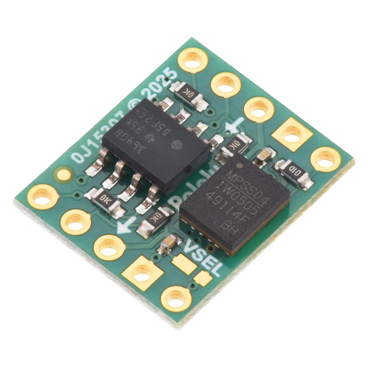
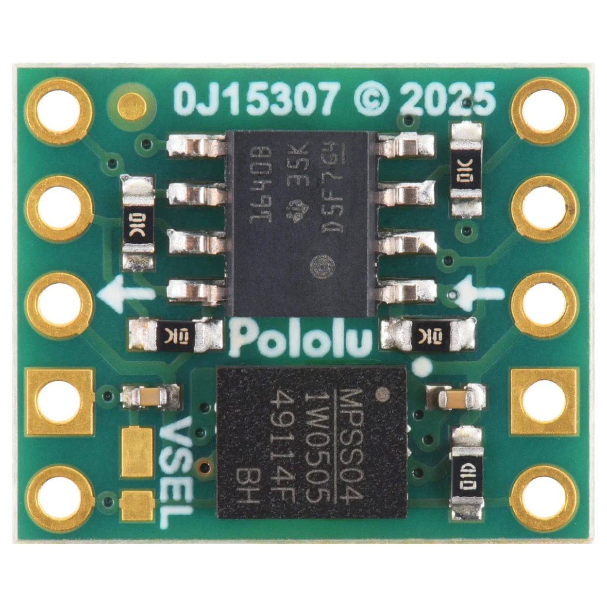
Pololu I²C Isolator with Isolated Power
This Pololu module enables galvanically isolated (electrically isolated), bidirectional communication between two I²C devices while providing isolated and regulated 5V or 3.3V power at up to 200 mA.
| Input voltage | Output voltage | Max output current |
| 4.5 V to 5.5 V | 5 V (default) or 3.3 V (selectable) | 200 mA |
| 3 V to 3.6 V | 3.3 V | 75 mA |
This isolation means that incorrect connections or bad voltages on one side cannot propagate through to damage the device connected to other side. The signal isolation is achieved with the TI ISO1640B, which supports bidirectional data transfer up to 1.7 MHz. See the ISO1640BDR datasheet for more information.
The isolated power transfer is achieved with the MPS MIE1W0505BGLVH. The output ground (GND2) is effectively independent of the input side, which can be useful for preventing ground loops and avoiding ground currents that can cause unpredictable system behavior or even lead to destruction. See the MIE1W0505BGLVH datasheet for more information.
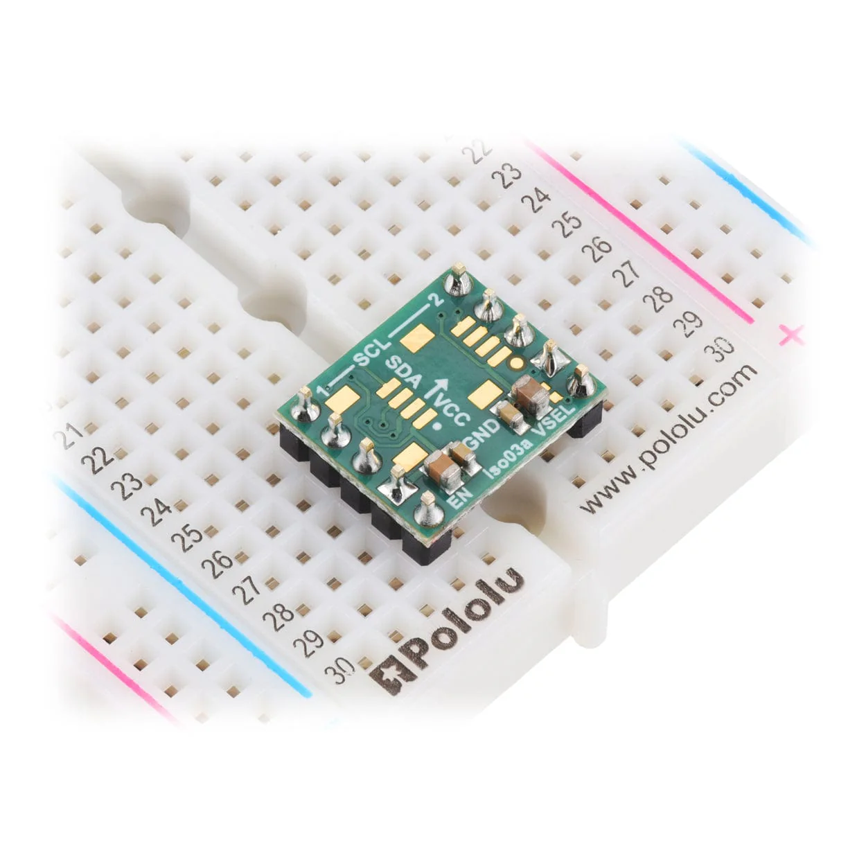
This is the version without connectors; connections are made via through-holes that are spaced with a 0.1″ (2.54 mm) pitch and compatible with 0.1″ male headers and solderless breadboards. We also stock a version with JST-SH (Qwiic/STEMMA QT compatible) connectors.
Features
- Galvanic isolation between the two sides
- Bidirectional SDA and SCL for bidirectional I²C communication with support for clock stretching
- 3 V to 5.5 V input voltage range
- Selectable 5 V or 3.3 V regulated output (5 V default)
- Up to 180 mA out continuous (200 mA peak) at 5 V in
- Up to 75 mA out continuous at 3 V in
- Over-temperature and short-circuit protection
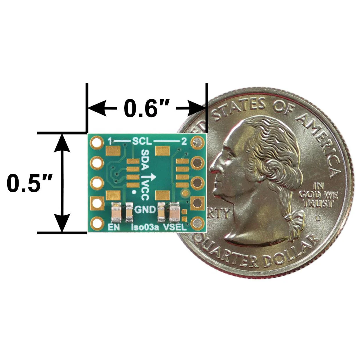
- Compact 0.5″ × 0.6″ size with breadboard-compatible, 0.1″-pitch through holes
Using the module

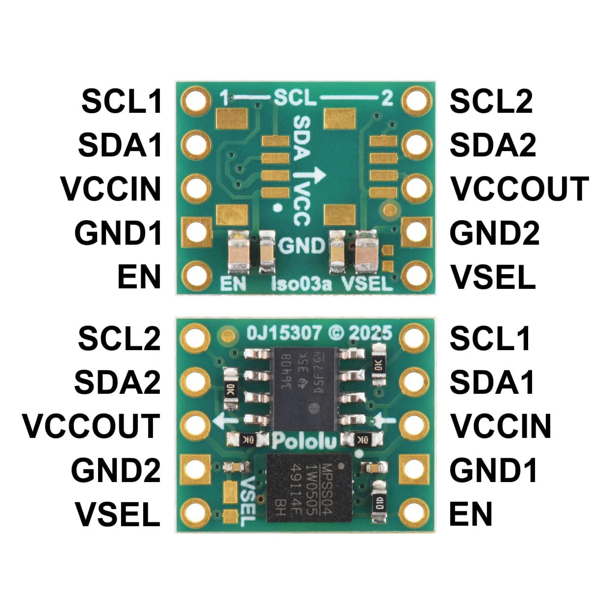
Input power is supplied across VCCIN and GND1 and output power is delivered across VCCOUT and GND2. The two sides are galvanically isolated (GND1 is NOT connected to GND2). Note that the efficiency of the regulator is less than 50%, so the input power will need to be at least twice the output power.
| VCCIN range | VSEL | VCCOUT | Output current |
| 4.5 V to 5.5 V | NC (default) | 5 V | 180 mA continuous, 200 mA peak |
| GND2 | 3.3 V | ||
| 3 V to 3.6 V | GND2 | 3.3 V | 75 mA continuous |
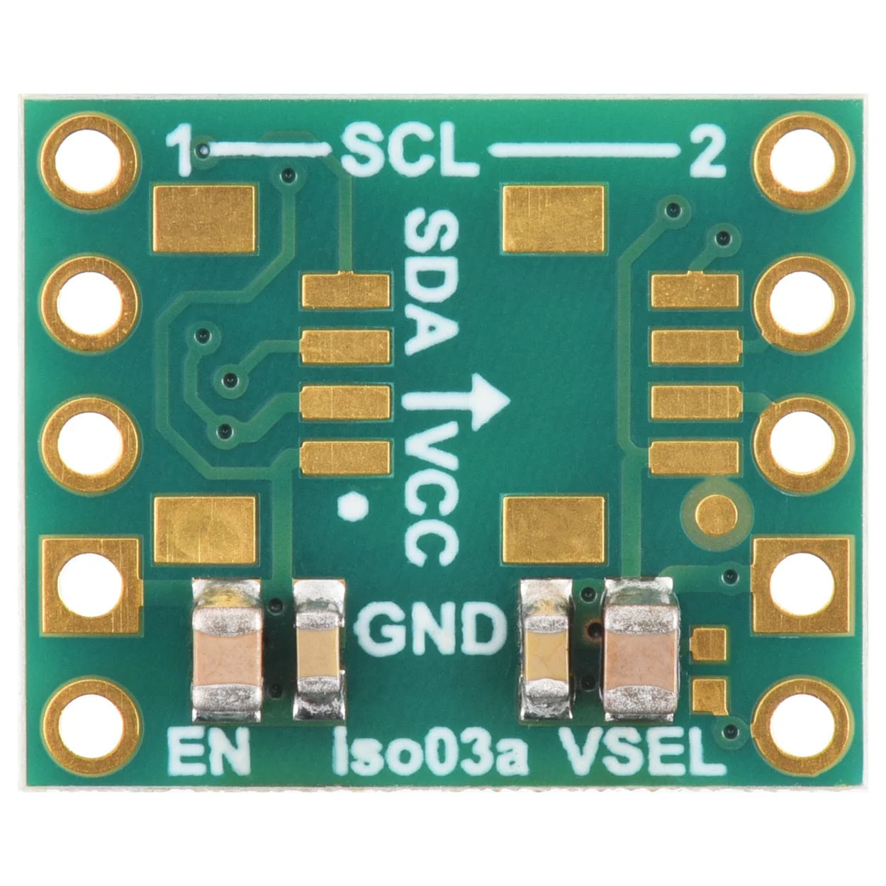
SDA1 and SCL1 connect to the I²C data and clock signals of one device while SDA2 and SCL2 connect to the I²C data and clock signals of the other. Both the SDA and SCL connections are bidirectional, which allows for clock stretching. There are 10k pull-up resistors from SDA1 and SCL1 to VCC1 and from SDA2 and SCL2 to VCC2; for high-speed communication, external pull-up resistors can be added in parallel as necessary to make the pull-ups stronger.
The enable input, EN, is pulled up to VCCIN through a 100 kΩ resistor, which enables the power transfer to the VCCOUT side by default. This pin can be driven low to disable the module and put it into a low-power state (note that the input side of the ISO1640 is not powered down).
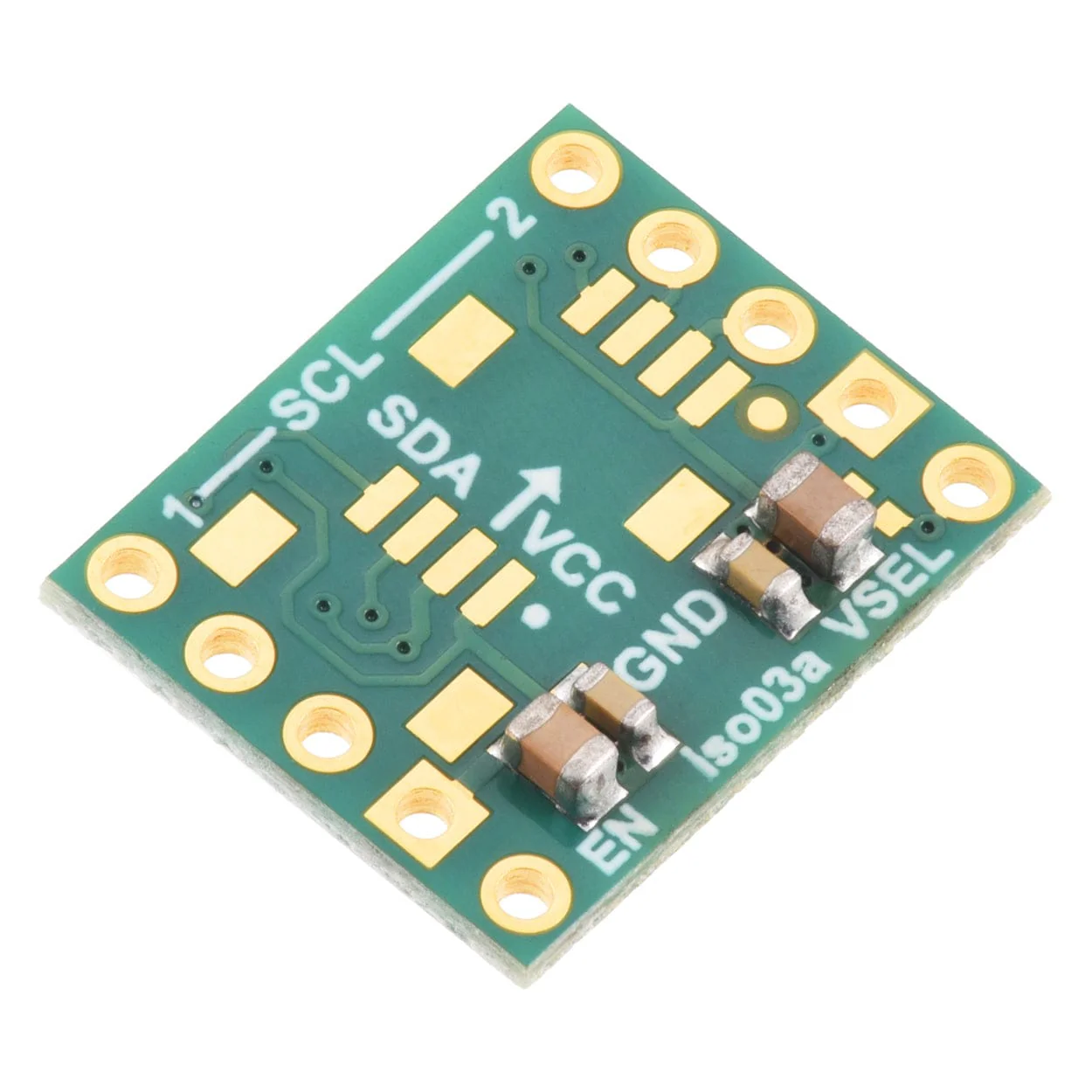
The output voltage selection pin, VSEL, is floating, which sets the output voltage to 5 V by default. To select 3.3 V for the output voltage, connect VSEL to GND2. This can be done using the board’s through holes (the left picture below shows an example of this with male headers and a shorting block) or by adding an SMT jumper to the pads circled in the image below. Note: Do not change VSEL while the regulator is powered.

Isolation/clearance considerations
Although the ISO1640 IC has an isolation rating of up to 3 kVRMS and the MIE1W0505BGLVH IC has an isolation rating up to 2.5 kVRMS, please note that the board is made to be compact, and the tightest clearance (2 mm) is smaller than clearances of the IC packages (4mm for the ISO1640 and 3.5 mm for the MIE1W0505BGLVH). The picture below shows the regions of tightest clearance (the larger pads are just structural pads for the connectors and are not electrically connected to anything):
![]()
Specifications
| Minimum operating voltage | 3.0 V |
| Maximum operating voltage | 5.5 V |
| Maximum output current | 200 mA |
| Output voltage | 5 V |
| Reverse voltage protection? | N |
| Connectors? | N |
| Isolated power transfer? | Y |
| Size | 0.5″ × 0.6″ × 0.11″ |
| Weight | 0.5 g |
Resources
- Schematic
- Dimensions
- 3D Model (STEP)
- Drill guide
- MPS MIE1W0505BGLVH datasheet
- TI ISO1640BDR datasheet
- MIE1W0505BGLVH MPS product page
Product Information
Product Information
Shipping & Returns
Shipping & Returns
Description
This Pololu module enables galvanically isolated (electrically isolated), bidirectional communication between two I²C devices while providing isolated and regulated 5V or 3.3V power at up to 200 mA.
| Input voltage | Output voltage | Max output current |
| 4.5 V to 5.5 V | 5 V (default) or 3.3 V (selectable) | 200 mA |
| 3 V to 3.6 V | 3.3 V | 75 mA |
This isolation means that incorrect connections or bad voltages on one side cannot propagate through to damage the device connected to other side. The signal isolation is achieved with the TI ISO1640B, which supports bidirectional data transfer up to 1.7 MHz. See the ISO1640BDR datasheet for more information.
The isolated power transfer is achieved with the MPS MIE1W0505BGLVH. The output ground (GND2) is effectively independent of the input side, which can be useful for preventing ground loops and avoiding ground currents that can cause unpredictable system behavior or even lead to destruction. See the MIE1W0505BGLVH datasheet for more information.
This is the version without connectors; connections are made via through-holes that are spaced with a 0.1″ (2.54 mm) pitch and compatible with 0.1″ male headers and solderless breadboards. We also stock a version with JST-SH (Qwiic/STEMMA QT compatible) connectors.
Features
- Galvanic isolation between the two sides
- Bidirectional SDA and SCL for bidirectional I²C communication with support for clock stretching
- 3 V to 5.5 V input voltage range
- Selectable 5 V or 3.3 V regulated output (5 V default)
- Up to 180 mA out continuous (200 mA peak) at 5 V in
- Up to 75 mA out continuous at 3 V in
- Over-temperature and short-circuit protection
- Compact 0.5″ × 0.6″ size with breadboard-compatible, 0.1″-pitch through holes
Using the module
Input power is supplied across VCCIN and GND1 and output power is delivered across VCCOUT and GND2. The two sides are galvanically isolated (GND1 is NOT connected to GND2). Note that the efficiency of the regulator is less than 50%, so the input power will need to be at least twice the output power.
| VCCIN range | VSEL | VCCOUT | Output current |
| 4.5 V to 5.5 V | NC (default) | 5 V | 180 mA continuous, 200 mA peak |
| GND2 | 3.3 V | ||
| 3 V to 3.6 V | GND2 | 3.3 V | 75 mA continuous |
SDA1 and SCL1 connect to the I²C data and clock signals of one device while SDA2 and SCL2 connect to the I²C data and clock signals of the other. Both the SDA and SCL connections are bidirectional, which allows for clock stretching. There are 10k pull-up resistors from SDA1 and SCL1 to VCC1 and from SDA2 and SCL2 to VCC2; for high-speed communication, external pull-up resistors can be added in parallel as necessary to make the pull-ups stronger.
The enable input, EN, is pulled up to VCCIN through a 100 kΩ resistor, which enables the power transfer to the VCCOUT side by default. This pin can be driven low to disable the module and put it into a low-power state (note that the input side of the ISO1640 is not powered down).
The output voltage selection pin, VSEL, is floating, which sets the output voltage to 5 V by default. To select 3.3 V for the output voltage, connect VSEL to GND2. This can be done using the board’s through holes (the left picture below shows an example of this with male headers and a shorting block) or by adding an SMT jumper to the pads circled in the image below. Note: Do not change VSEL while the regulator is powered.
Isolation/clearance considerations
Although the ISO1640 IC has an isolation rating of up to 3 kVRMS and the MIE1W0505BGLVH IC has an isolation rating up to 2.5 kVRMS, please note that the board is made to be compact, and the tightest clearance (2 mm) is smaller than clearances of the IC packages (4mm for the ISO1640 and 3.5 mm for the MIE1W0505BGLVH). The picture below shows the regions of tightest clearance (the larger pads are just structural pads for the connectors and are not electrically connected to anything):
![]()
Specifications
| Minimum operating voltage | 3.0 V |
| Maximum operating voltage | 5.5 V |
| Maximum output current | 200 mA |
| Output voltage | 5 V |
| Reverse voltage protection? | N |
| Connectors? | N |
| Isolated power transfer? | Y |
| Size | 0.5″ × 0.6″ × 0.11″ |
| Weight | 0.5 g |
Resources
- Schematic
- Dimensions
- 3D Model (STEP)
- Drill guide
- MPS MIE1W0505BGLVH datasheet
- TI ISO1640BDR datasheet
- MIE1W0505BGLVH MPS product page